

◆Applicable to semiconductor photolithography, inspection equipment, and optical masks;
◆A variety of materials are available for selection;
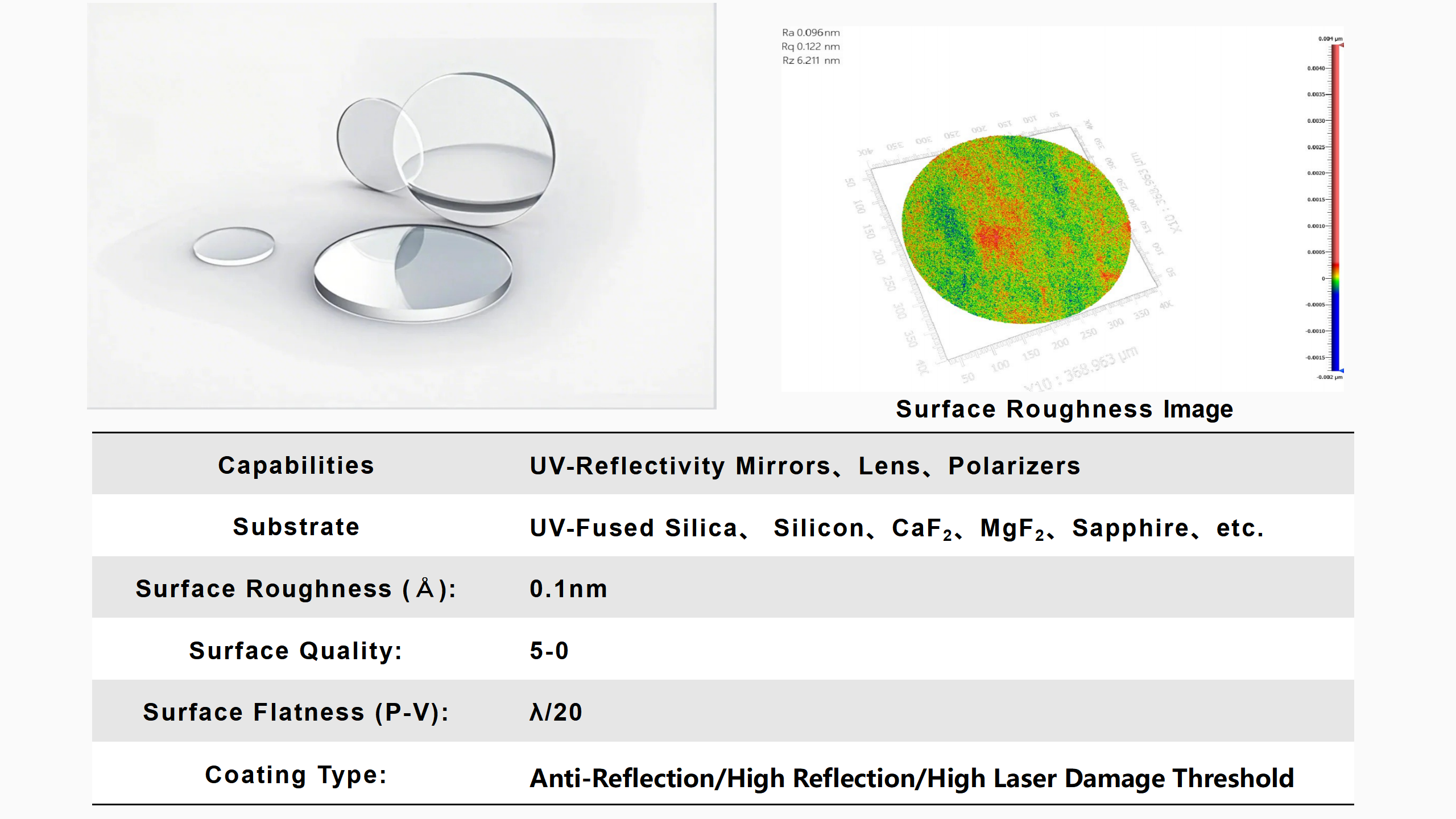
◆Surface Roughness (Å) is better than 0.1nm
◆Supports small batch customization
◆Applicable to semiconductor photolithography, inspection equipment, and optical masks;
◆A variety of materials are available for selection;
◆Surface Roughness (Å) is better than 0.1nm
◆Supports small batch customization
